Thursday, May 19, 2011

Pioneer DV-500 SMPSU Repair

Pioneer DV-500 that wasn’t powering up arrived on my bench one morning. Managed to diagnose it down to the SMPSU being dead. Forgot that I’d left my trusty DMM at my workplace, so I hauled it over to the shop to get it fixed.

I found a slightly different model’s service manual floating online, but it utilised a close enough power supply that the schematic and board layout were almost a 1:1.

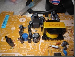
Here’s a shot of the power supply. Those are some good quality capacitors they’ve put on there.

IMG_0962

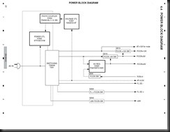
The standby voltages were ultra low (1v for a usually 3.3v supply), and was oscillating. In the service manual there was a block diagram, some troubleshooting flowcharts as well as the full schematic.

Pioneer DV-300-K (RRV3584)_Page_22

Pioneer DV-300-K (RRV3584)_Page_23

I checked everything around the 3.3v supply and couldn’t find anything wrong, the main controller IC was getting the right amount of voltage from the bias winding (around 13V), was scratching my head for abit and then decided to test everything to see if something was shorted, causing the PSU to not come up.

Very quickly I managed to find a shorted secondary rectifying diode, it was on the 5v line, I desoldered it out of the circuit and confirmed it was a dead short, these things are known to fail.

IMG_0965

I repowered the PSU, expecting it to come back online since regulation was done on the 3.3v rail, but no, the bugger still wouldn’t come on.

This was when I decided to give up on the block diagram (it wasn’t showing everything) and use the schematic. Finally it became clear that there was protection on the PSU that prevents the outputs from coming live if any rails had low or missing voltages.

Pioneer DV-300-K (RRV3584)_Page_60

PNP transistor Q506 prevents the power supply from fully coming on if the voltage at the base is lower then the emitter, the emitter’s voltage in this case is regulated by zener diode D523 to around 3.6v, so anything lower then about 3.0v will cause it to conduct and through the optocoupler, shutdown the supply.

In this case the base is indeed lower then 3v, about 0v in fact, due to the missing 5v rail. Once I figured this out, I tried lifting one pin of D522, which ‘feeds’ (can’t really say feed here, it’s more like leak), to the base of Q506.

IMG_0963

That finally made the power supply start up, and the other rails measured good, confirming that the shorted 5v diode was the only bad component. I couldn’t located an exact replacement, so I dug one out of an old PC PSU (which is a lot beefier then it really needs to be on this PSU).

IMG_0967

I put some heatshrink on the metal tab of the diode, to prevent it from shorting against anything on the board.

IMG_0968

Here it is in it’s new home.

Pieced the entire DVD player back together.

IMG_0969

The DVD player uses a Mediatek 1389 SoC to do all the decoding, pretty famous for it’s DVD-VIDEO, DVD-AUDIO, Super Audio CD, DivX, WMA, WMV, JPG, MP3, and MPEG4, as well as its high-quality Pal-to-NTSC and NTSC-to-Pal conversions. Ah well, blu-ray is all the rage nowadays.

Anyways it works properly now, –1 DVD player in the landfill.

IMG_0970

Xbox 360 Xclamp replacement.

The Xclamp is Microsoft’s weird heatsink retention mechanism that puts undue stress on the Xbox’s motherboard, leading to warpage and then finally the solder under the GPU/CPU gives way and then you get an RROD. I’m replacing that with a couple of screws and washers to prevent board warp.

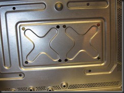
1st you’d need to enlarge the stock screw holes on the chassis to 5mm dia to get the new screws to fit.

IMG_0974

Then you’d need to get hardware to mount the whole thing on. You’re gonna need a couple of M5x0.8x16mm screws and 1mm thick washers to get the dimensions right.

After getting all the hardware, take off the stock retention studs on the bottom of the heatsinks, and also cut away and flatten the stock Xclamps.

IMG_0973

Once done, start putting in the hardware.

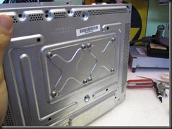
IMG_0976

I use some tape to temporary prevent the screws from falling out when I tip the chassis over.

IMG_0978

The flattenned Xclamps go on, and then enough washers to make up 3mm height.

IMG_0979

A piece of 4mm foam underneath provides support around the CPU and GPU area.

IMG_0981

Put in the heatsinks and lay the Xbox on it’s side, then tighten the fasterners, in a cross pattern to exert even pressure.

IMG_0980

Once done, put together the Xbox as per normal.

Credits to http://xbox-experts.com/tutorial/team-hybrids-ultimate-xclamp-fix-released/ for giving me this idea in the 1st place.

Sunday, May 15, 2011

Repairing RROD Xbox 360 Xenon

Most people will consider the Xenon (early Xbox 360s with no HDMI) a waste of time and not worthy of repair, however this unit had an early dashboard/kernel that could be JTAG’d, so saving it had some merit.
1st thing I did was to reball the original GPU, however upon attempting to remove the GPU, I pop-corned it (delaminated the GPU), even though I had already prebaked the entire board at 100deg for over 7hrs, wasn’t using a too fast ramp up and wasn’t too close, I ‘m putting it down as way more moisture in the BGA package then I anticipated (Xbox was dis-used for awhile and here the humidity is amongst the highest you’ll find in the world).
Pulled the GPU and bought a couple of spares, they arrived nicely in the tape+reel packaging and already pre-balled with leaded solder.
GPUsBalls
Prepped the board (wick and clean it out real well, then apply some flux), this time I’m trying a generic liquid flux that I got locally (mostly IPA with some rosin based flux in it).
Board
The soldering process went pretty uneventfully, here it is completed. The flux does leave behind some pretty heavy residue, might be because I used way too much.
Heating GPU
Down
Cleaned off the residue with some IPA, and then tried to boot the box up. Expecting it to work 1st go, but no dice, it RROD’d again with a secondary error code of 0022. I was scratching my head for awhile, and then I tried reflowing the GPU again (thinking it never attached properly or something) but still 0022.
Careful visual check on the bottom side of the board though, I found this.0022
So apparently one component had moved and was creating some kinda short (I believe it’s a fuse or a 0 ohm link). Moved it back into place, and then again expecting the Xbox to work, no dice, 0102 error code now.
SB reflowing 0102
I reflowed the SB and rams around the GPU, but still no dice. Again careful inspection helped out, I noticed a very small air pocket starting to form on the top side of the GPU, must’ve happened during the 2nd reflow (I tried slightly higher temps). Ah well…
The next GPU I attached underwent a 2hrish bake @ 125 to try and get rid of moisture, and this time I used the fake Amtech flux (read my previous post for more info) to attach the GPU (I find it less messy due to the more controllable quantity, liquid flux is kinda hard to quantify). Tried booting it up after it’s cooled down (without moving the board too early this time, I think that was what made the component moved previously, although why only 1 moved it beyond me) aaaannnnndddd…….
FINALLY
SUCCESS. I’ve yet to properly test it out over some time though. Will apply an X-clamp replacement 1st and then go on from there. That’s another update though. If you're interested in getting your Xbox fixed, or looked at, visit http://www.epicgear.com.sg/.

Wednesday, May 4, 2011

Fake Amtech RMA-223-UV Flux

Noticed this recently on my tube of flux that shipped with the machine. Was already super dubious about it’s origins (It had huge MADE IN USA labeling on it, and yet shipped from China.)

Abit of searching online led me to this site.

http://ultrakeet.com.au/index.php?id=article&name=fluxInfo

Where the poster had bought on DX (DealExtreme) and Ebay, flux of dubious origins and confirmed with Amtech that there were indeed not original products.

Here’s a couple of photos of mine.


3004201102830042011031

Notice the mis-spelt Colifomia.

While RMA-223 is just a type name, rosin mildly activated, EN 29454-1 type 2.2.3. I don’t like the fact that they are trying to use Amtech’s name to get it to sell.

It’s bloody cheap on Ebay and DX too, like $2 for 1 tube, while the real stuff is usually 10x pricier, so I guess you get what you pay for.

As for the flux performance, I actually find it surprisingly good, better then the rest of the stuff I have on hand at the moment, very little moisture content (low bubbling when heated), adequate tackiness for my reballing applications and good wettability, I haven’t got the real stuff to compare against, so I can’t tell you if it performs the same. It’s not a no-clean formulation so you have to clean it off, I have found that it leaves a whitish residue that may screw up your high frequency stuff, but my cleaning solvents (IPA and/or limonene based cleaner) works real good on this.

The problem though is consistency, there is no date stamped on the tube and I don’t suppose the QC is even existent, so no idea if the next tube will perform the same as this one. If I ever get another tube just to find out. I’ll post more information.

Tuesday, May 3, 2011

Taking apart a Mac Book Pro 15” Battery Pack. Part 1.

Had a battery pack with bad life, pack could still hold a charge, but the runtimes were seriously degraded (1hrish). Decided to re-new the cells instead of throwing away and buying an entirely new pack.

Not much information on the net about people doing this. DO NOTE THAT THE CELLS ARE LITHIUM POLYMER TYPES, PUNCTURING AND/OR DAMAGE TO THEM CAN/WILL CAUSE A FIRE. Still decided to do it though.

To expose the cells. You’ve gotta remove the top aluminium sheet that’s mounted with a very sticky tape. Start at the corners and go slow, applying some solvent (used IPA for this, seemed a good idea), there’s a thin metal cover between this and the cells, so you shouldn’t be able to start a fire unless you’re seriously using a lot of force. The button and LEDs are not part of the cover. (Button is simply a little metal thing that extends all way down into the controller/protection PCB.)

30042011026

With the cover out you’ll see yet another metal plate, lift the corners and work your way around it’s mounting tabs. There might be some adhesive on the tabs, gently get those off.

30042011027

With that out, next gently remove the little cover just above the power connector, doing this will free the board and cells enough to get them to move. Then with gentle persuasion, guide the cells and board out.

30042011024

30042011025

Next up in this series, replacing and then finally putting the pack together.

Monday, May 2, 2011

Reballing a GeForce 8600GS

Needed to test out if my skills and profiles are all correct for a good reball. A good way to do this is with old hardware.

Before doing this though, I had already attempted to reball a GeForce 4 MX 400, but that was easier as it was using leaded solder (183deg melt point) thus giving me more room for error (more room between package max temp and solder melt temp.) Unleaded solder (depending on the specific alloy used, usually starts melting at 217 and completes melting around 240ish.

It’s a good idea to pre-bake your stuff if it’s been left unpowered and out in the open to collect moisture, any amount of moisture will decrease your chances of success due to package delamination, the moisture tries to escape during heating and creates a bubble in between the BGA layers, not cool.

Anyways, here the pictures and process involved. I preheat my board at 135ish for about 3mins before proceeding.

29042011008

Here’s the card after the main GPU has been removed, thermocouple position during this process is quite important, you need to make sure it’s contacting the board 100% of the time, otherwise the readout will not be consistent. I pre-flux the board with Amtech RMA-223-TPF-UV (UV reactive tacky paste flux), this flux seems to work pretty good.

On the top left corner, sharp eyed readers might notice a popped capacitor, the card actually was working fine with this defect, really weird.

29042011009

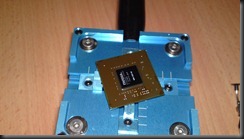
Here the main GPU die is resting after being sucked out, I use a cheap vacuum pen.

29042011001

And then here it is again, mounted properly in the jig to facilitate removal of the existing solder balls.

I usually leave the bottom heat on the PCB on, and then go ahead to clean up the board 1st before doing anything else. I reball with Sn63 Pb37 solder.

29042011014 (2)29042011013 (2)

To clean it up, I flood the area 1st with leaded solder, hoping to replace most of the unleaded with leaded, then move the dross out of the way, before cleaning it all up with solder wick and then a solvent clean.

Next I tackle the BGA package.

29042011002

Again I flood the area with leaded solder and move the dross out of the way when I’m done.

29042011003

Then I use wick to clean everything up, being generous with the wick I ensure the solder is completely removed, any residue will increase the chances of solder bridging later when I put in the balls.

29042011004

Next I put it in an ultrasonic solvent bath to remove all traces of flux, the flux I’m using is NOT a no-clean formulation.

2904201100729042011005

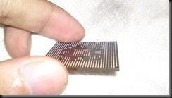
This is what it looks like after a good clean and wipe down.

29042011009 (2)

Next I select an appropriate stencil, and give the chip a thin coat of flux, then position the stencil over and press it down. The paste flux should hold it in place, but it can still slide a little around, to prevent that, I tape the back with a small amount of aluminium tape. Then I proceed to put in the balls.

2904201101029042011011

Here it is balled. I just hold the stencil + IC package over a small metal bowl, and flood the top with balls, then gently shake and swipe the excess away. The stencil I am using is not an exact for this IC, but it’ll be close enough (excess balls around the side, which can be removed later).

Next I place it ontop of the jig, and move it over to the IR station for heating.

29042011012

Here it is undergoing heating, I use a leaded profile, with a head set to about 3.5mm off the IC, and then the thermocouple UNDER and TOUCHING the BGA.

After this is done, I apply a small around of solvent on the circumference of the package to try and get it in between the stencil and IC, sometimes it can get stuck on pretty bad. Then I inspect for any missing balls, and re-work if necessary. The balls are 0.5mm in dia, so not too difficult to put them in manually. After I’m satisfied, I clean it up again in the solvent bath.

29042011015

This is the package after being re-balled and cleaned.

Last step is to attach the 2 together, a thin layer of flux is applied to the PCB and the reballed package is carefully aligned on top. Then I go through the process of pre-heating and then reflowing (now to 185deg instead of 240) to get the leaded balls to melt and fuse with the PCB.

29042011016

29042011017

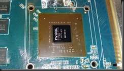
Here it is, done.

29042011019

I then visually inspect around the edges, making sure the balls have made a good joint, you can’t see inside, but that’s just the way it is, unless you fork out some $$$ for an X-ray machine.

29042011020

After slapping on the heatsink (applied some paste), hey hey, the card boots fine. Success =P. I later replaced the defective capacitor on the card and it’s now in use as a test card, since it just refuses to die.