Sunday, May 15, 2022

Kenwood KA-691 repair

Unit received in fair condition, front looks good, no deep scratches or missing paint, rear and bottom has very slight corrosion.

Unit will not come out of standby mode, cut bottom chassis for service access, found no issues with main amp board.

Powering up microcontroller (front panel assembly, MCU is a M50941-597SP), was able to get some response from VFD with CD DIR depressed. Leaving it powered up for a couple minutes does eventually result in normal amplifier operation.

Took the chance to check output offset (negligible) and re-adjusted bias for 18mV per service manual.

Pulling power off and allowing amplifier to cool, will mean the next round of power up will take minutes for amplifier to come out of standby, verified clock to MCU is correct and started, Vcc and AVcc were correct and present, tried external 5V regulator, changing input filter caps, trying a quartz 4Mhz crystal instead of original resonator, to no avail, slipped DMM probe and shorted MCU pin from -35V (VP/VFD bias voltage) to adjacent input pin (38 shorted to 39 or 37). MCU now real and truly dead (heard a small pop and immediately shut off the amp by pulling power cord out).


Bad MCU

Opps, killed this little sucker.


Was unable to located MCU (PN M50941-597SP or M50941-589SP) even through obsolete component brokers/traders. Decided to cannibalize from another unit (got off eBay USA).

Rear inputs slightly polished to assure good shield contact, input board was removed for visual inspection.

Re-soldered power input board where joints showed signs of crack formation, re-soldered main amp board as well.


Cracked oxidized joints on main board

Cracked and oxidised joints on main PCB.

Joints reworked before cleanup

Reworked these

More inadequate joints

More inadequate joints

Board cleaned up

Main PCB cleaned up after rework.

Signs of crack formation transformer

Signs of cracking on transformer ribbon

Reworked transformer joints

Joints reworked

One reworked joint on transformer output

Reworked one joint on transformer input.


Service access panel flipped and re-attached with M3 washers and screws.

Speaker A & B switches cleaned and lubricated.

Ebay amplifier arrived in broken condition (likely due shipment damage, tone control’s smashed, power button smashed, will not turn on), returned.

Seller agreeable to sell just the front panel PCB for parts, procured front panel PCB alone.

PCB arrived, wrapped in aluminum foil and plenty of bubble wrap for ESD and shock damage resistance, front power switch PCB area found cracked and power switch pushed in.

Switch PCB patch

Crack stop drilled and PCB trace patched.

Top side patch

Epoxy patch on front of PCB.


ESR measured on all front panel PCB capacitors. Qty 4 were replaced as follows

Designation

Original values

Installed values

C80

220uF 6.3V Low Profile

220uF 10V bent over

C92

220uF 6.3V

220uF 10V

C89

10uF 50V

10uF 50V

C83

10uF 35V

10uF 50V

Power switch desoldered, new power switch soldered, cracked PCB trace patched over with enameled wire, crack stop-drilled with 1/16” drill bit. Solder side PCB lightly sanded and epoxy applied over cracks, top side sanded and a small patch applied with epoxy as well.

Power ribbon pads on front panel PCB slightly damaged during removal (qty 3), post soldering power ribbon connection, extra 3 enameled wires were used to jumper over to the ribbon connections and held down with Dow Corning 3145.

Ribbon patch

Jumper wires on front PCB


Unit tested and verified to power up instantly upon application of wall power.

Monday, April 25, 2022

O2 Headamp output board, OPA1688s Part II

It’s been awhile since I’ve had an update on this project, I actually completed it, but never got around to documenting everything.

Drew up a schematic and layed out a board, JLCPCB fabricated it with no issues. I used some existing board images that AGDR made available, so mechanically it’ll fit and clear whatever the O2 has existing on the board.

PCB


A set of 2 mil-max pin headers are used to interface to the existing opamp sockets, and then a couple of jumpers are required to tap onto the existing O2 board (ground, signal ground and lastly for the battery voltage comparator).

1 Channel

Each channel again is a bunch of OPA1688s paralleled (see previous post here for details) The Danger Zone: O2 Headamp output board, OPA1688s Part I (fillwithcoolblogname.blogspot.com)

Soldered

Here it’s partially assembled, I use liquid flux (that’s kinda messy). Everything gets dunked in my ultrasonic cleaner afterwards though so I’m not worried.

Rear

View of the rear, there’s an output relay that latches and prevents that annoying O2 issue of dropping in and out when battery levels get low and creates that popping noise (which is probably not good for your headphones).

Jumper 1

From the front assembled, here the signal ground jumper is visible.

Jumper 2

Top assembled, here the comparator jumper is visible.

Jumper 3

Last jumper for power ground, straight to the battery holder.

Offset 1Offset 2

Offset voltages measure pretty good.

Capacitive load test

I stacked a whole bunch of capacitors on my breadboard to do some random capacitive loading tests (with a ~33ohm) load, it performed admirably (I can’t exactly remember the numbers, I think it was 2nF or so load capacitance with 33Ohms, typical headphone cables are maybe 30pF per foot, so this is plenty stable). 


Top view

Finally this is it all assembled and cleaned up.

I haven’t gotten around to putting the schematics and board diagrams anywhere. If somebody is interested I’ll get off my ass and do it. Myself I’m fairly interested in what this measures properly in terms of THD+N, but I don’t have access to any cool equipment to do it. Smile

Saturday, April 16, 2022

Spectra S1+ Not Charging Battery

Had another unit to mess with. This will not charge it’s battery, upon power on with the charger/adapter, the battery icon blinks empty continuously for abit, before it gives up trying to charge the battery.

Turning the unit on without the adapter, the LCD will come up for 1 sec, then shutoff.

Took it apart, battery looked fine, voltage measured ~11.1V and stable (I thought it was dropping out when the pump was commanded to run), pulling the pump and solenoid connector off and trying to run the unit with the battery, exact same behaviour (shut itself off after 1 sec).

I then turned my attention to figuring out how the microcontroller on board measures battery voltage, found a resistor divider and a little output capacitor just to the right of the microcontroller (R36, R38 and C35R).

Measuring the top (input from battery) and turning on the unit from the front panel (fiddly yeah), I only measured ~8V (when it should be ~11V), somehow full battery voltage was not making it through. The input is not applied to the divider all the time, only when the micro commands the unit on, does input voltage appear thru the action of Q12, Q11 and Q9. Patch jumper

Probing around Q12, Q11 and Q9, I couldn’t find anything wrong with them. I ran a jumper from battery voltage to the input of the voltage divider and verified the unit works as it should, next I shifted the jumper to the input of Q11 and once again verified that the unit works (will accept charge, will turn on and stay on with battery power).

This was when I realised there might be some broken trace or via from battery voltage to Q11.

Flipped the PCB around and removed the LCD+plastic support.

Looks like some damage

Looks like some fluid damage under the Down switch.

Switch liquid

I removed the switch, cleaned the mess up and found that a via leading to the other side had broken, there’s no good way to patch that via (since it’s so small) and I opted to keep the jumper on the component side. Didn’t take a picture of the completed patch, but it looked like the original jumper I put on, except tucked neatly away and the battery voltage tapped from closer to the battery connector (after the ferrite bead from the charging section).

Reinstalled everything, charged the battery and tested it out, I can confirm everything is working as it should. Smile

Saturday, April 9, 2022

Spectra S1+ Repair

Received one that wouldn’t turn on even with the adapter plugged in. Unit opens up with 4 screws removed from base.

Quick check found the main power rail shorted, initially I thought it was a shorted TVS on the input, removal of the input TVS didn’t fix that, so I started looking around, that’s when I found a small burnt area on the PCB.

Burnt out FET

Towards the left is the burnt out component, nearby is a NCP3063, as far as I can make out it’s a boost converter (I didn’t know initially what it does until later). I couldn’t de-solder the FET normally as it had fused itself to the PCB track when it failed. Applying heat and leveraging it off the board the copper it was soldered onto de-laminated from the PCB itself. Luckily the source and gate pins came off the PCB ok (just the drain pins were affected).

As far as I can tell, the SMD markings point to the FET being a NTGS4141N (S4 marking code, 7 date code).

With the FET removed (I cut the dangling bit of the PCB off with a scalpel), I could actually power up the unit with the adapter plugged in (yeah!).

I then decided to check if the FET driver and NCP3063 were at least still operational.

FET removed Drive check

Hooked up some insulated magnet wire to the drive to my oscilloscope.

Drive Waveform

That verified it was still working, also during this time I saw the drive only come on for a couple secs during initial power up, my guess is it’s used only during battery charging (the pack is a 3S 11.1V nominal battery, so it needs ~12.5V to charge it fully when the adapter only outputs 12V, and charging is done through a MAX1873, which I guess needs a couple of volts headroom to charge to ~12.5V)

Scrounging around in my parts bin I found a NTP18N06, which is fairly similiar in terms of drive requirements, but a little higher Rdson (90mOhm vs 21.5), since I had lost part of the PCB I figured the exposed TO220 package would probably be best for heat dissipation and there was ample room on the PCB to mount it on.

Old Vs New

Yeah, the size/packaging difference is huge.

Tacked in for sanity check

A quick solder job and viewing the drive on the oscilloscope + output voltage measurement, verified nothing was wrong, no smoke and the boost circuitry output voltage was present (~14.5V or so for a couple of secs, I tried hooking up the original battery pack to see if it’ll start charging and let me test this section for longer but the pack was too far gone).

FET placement final

I scraped off a bit of PCB on the ground plane, flipped the TO220 package around and soldered the source pin directly to the FET, ran some insulated magnet wire to the inductor and gate pin on the PCB, held everything down with Dow Corning 3145 (electronics safe RTV).

Next I turned my attention to the battery pack, which had a bloated LiPo cell, I couldn’t source an exact replacement 3S battery pack (it uses a built in BMS to balance the charge, there are only 2 wires coming out of the pack, so non of the usual RC type LiPo packs with external balance connectors will work safely, at least not without wiring up a BMS on it). I removed the bad cell from the pack and clipped a random partially charged 18650 to it, attempting to charge it the battery came back to life (the BMS had stopped any voltage from coming out the pack with the 1 bad cell)

Swollen LiPo

Got my hands on 3x new Molicel P26A 18650s and I decided to keep the original BMS.

Battery Test

A bunch of spot welding and soldering later, I’ve got a working battery pack with the original BMS.

Battery Replaced Final

Here it is in it’s original spot. I’ve elected to tape the original labels within the machine in case somebody/someone else needs to know what was in it originally. With these new cells, I’ve verified it’s able to charge and stop properly, (cut off at 12.5V) and it should last a bit longer given the capacity has now increased (original 2000mAH, now 2600mAH).

Finally, I re-soldered the input TVS diode and closed it all up. 😁

Saturday, February 12, 2022

Mackie CR4 Repair

Over the years I’ve replaced all their internal capacitors, changed out the 12V zeners in the regulator area for beefier units (the stock ones are down on the PCB and keep dumping heat into what appears to be cheap PCB material, it’s definitely not FR4, I tried mounting them off the board to give it room to dissipate the heat), also had replaced the L-R switch and scrapped off all the nasty glue that they used during manufacture that was turning conductive and corroding components on the PCB (I saw a resistor lead almost disintegrate to nothing).

Right now they will come on, but will randomly get muted, I suspect there is even more damage to the 12V regulator area on the PCB and the mute circuitry was kicking in on the TDA6275 (all kinds of guides exist on the internet that just tell you to snip the Mute pin off, it’s not a proper fix as the Mute circuitry ensures +/- 12V exists before unmuting the amp section).

Regulator

That’s the 12V section, after removing the associated components.

Burnt PCB

The PCB after I’ve cleared off the tracks that were heat damaged, it’s too far gone to try to patch up. During the process I found a cracked trace on a leg of a zener diode, that was probably why it was randomly muting.

I decided to remove all the circuitry around the +/-12V area, including the components that generate the mute signal and move it all to an external PCB.

The original +/-12V regulation was achieved thru value engineering with the below

Reg Ori

The mute was done as below (I’d have to replicate this on my board)

Mute Sch

Drew up a schematic and layed out a board. I’ve used TO220 7812 and 7912 for the regulators and all through hole parts.

Sch

PCB

Here it is populated and installed.

PopulatedInstalled

A picture of the clearances and mounting involved (I used a single mount point in between the 2 TO220 regulators, I wasn’t sure the PCB would be ok flapping in the breeze inside the speaker with just the TO220s for mechanical support).

Mount and clearance

And the rear of the entire PCB when I was done, I’ve marked out where the +/- voltages get tapped for this external regulator+mute board as well as where the +/- 12V regulated voltages go back in. I’ve left the burnt area as is (didn’t attempt to grind them out) but with a sharp scalpel cut off the tracks back to a good area, so nothing is shorting.

Back

Putting it back together, I can confirm they work, time will tell if they keep working.

Monday, December 14, 2020

O2 Headamp output board, OPA1688s Part I

NwavGuy left us with a fairly well performing, battery powered headamp. I built mine fairly early on when they got out into the wild.

It's been almost 8 years since he disappeared into the ether and in that time, plenty of new opamps have been released which seemingly (at least on the surface) look like a better deal then the NJM4556s that drive the outputs (lower distortion, offset as well as higher output current capabilities).

Nwavguy himself was fairly certain the output opamps were the bottleneck for the O2's THD figures, AGDR attempted an output booster that was based on LME49600s and OPA827s (Around 14USD in opamps per channel).

https://www.diyaudio.com/forums/headphone-systems/244473-o2-headamp-output-booster-pcb.html

Ultimately I feel that the LME49600s were difficult to heatsink properly given the tight internal space. I do indeed think it should provide (at least for a limited time) way more power than the original 4556s were capable of, the headphone mute relay addition is also a double bonus (rid turn on/off thumps and the motorboating thing that happens when the O2 batteries get drained). 

Unsatisfied I went around looking at Opamps released fairly recently. There were 2 that caught my eye.

One of them would be the OPA1688, the other would be the OPA1622. 

Decisions, 1688s doesn't quite have the capacitive drive, the 1622 is in a tiny package that's a pain to solder and bias currents are ~1.2uA, meaning I'd need another opamp stage in front of the 1622 to drive it properly. 

I decided that parallel 2x OPA1688 (4 op amp channels) would be my design choice, my lowest impedance headphones are 32 Ohms and some back of the envelope calculations determined that even at worst case dissipation, the opamps should scrape through and not hit Tj limits. The O2 is/was all about getting performance at a lowish cost, which I think this decision would be in-line to.

External compensation  by increasing noise gain to improve phase margin was figured out with inputs from johnc124 for another project.

https://www.diyaudio.com/forums/headphone-systems/293247-opa1688-super-cmoy-2x-9v-real-ground-headphone-relay-pcbs-7.html#post4762471

Power dissipation calcs:

RL = 32R

Parallel 4 = 128R effective

Pq = 24(0.018)

     = 0.0432W

Io = 6/128

    = 0.046875W

Pdmax = 6(0.046875) + 0.0432

            = 0.32445W

Temp rise over ambient = 0.324(116.1)

                                       = 37 deg C (per opamp)

                                       = 75 deg C (per SOIC dual opamp device)

To be continued in Part II

The Danger Zone: O2 Headamp output board, OPA1688s Part II (fillwithcoolblogname.blogspot.com)

Monday, October 26, 2020

Klipsch Promedia GMX 2.1 Hiss & Weak headphone output

Klipsch made some questionable choices with regards to the amount of gain and how they drive the headphone outputs. Mine had bad volume and sub control potentiometers so since I was gonna dive in and replace those, I might as well fix the hiss and headphone section.

Per the stock design, there's an insane 7.5 gain (just on the headphone section) regardless of where the volume control position is at, even with it off, which just makes the speakers hiss constantly (I can hear them at my sitting position) even with no / grounded inputs, I have never used the volume control past the 1/4 mark.


I've traced out just headphone section (bottom right of the control pod PCB), which is the biggest contributor to this hissing. No idea why they went with output resistors and 7.5x gain, with such a insane amount of output resistance the voltage driving the headphones just gets dissipated in them. I put in 1kHz sine wave and measured ~120mVp-p but only ~50mVp-p on the headphone side of the resistors. 

Here's what I did to fix all that. In the course of messing with this I killed the PT2308 while probing around (opps), they're kinda hard to come by in a DIP package, so I was either gonna have to put one on a SMD converter board or put a different opamp in there.


I went with a NJM4556 (which has more output current capability than the original), a gain of 1.5 (which was plenty loud on my headphones), removed and shorted out the 2 output resistors, increased the output capacitors to 470uF, upped the input capacitors to 6.8uF (probably overkill) and changed the feedback capacitor to 150pF (prevents HF from being amplified). 

Even with the stock 33pF feedback capacitor, I didn't manage to get the opamp to oscillate. A good test is probably to stick a nice sharp square wave onto the input and see if it's gonna ring a bunch, I might do that if I experience issues. 

With the changes in place. I can only hear a slight hiss if I place my ears right up to the speakers and only from the tweeter. I no longer have to only use the bottom 1/4 of the volume control and I get plenty of drive to my headphones. I'm happy, lol.

Monday, September 17, 2018

ECU repair Miata NA8 1996

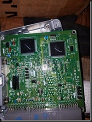
Miata NA8 1996 ECU repair, car wouldn't start, swapping in a 2nd ECU and it started.

ECU1

ECU out of it's case and my trusty DMM.

ECU2

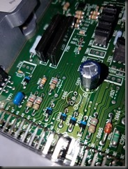
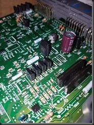
ECU overview, as far as I can tell there are only 3 electrolytic capacitors.

ECU3

C006 has developed a nasty leak and spilled some of it's guts on the board.

ECU4

Cap removed, some of the conformal coating around that area was damaged by the capacitor electrolyte.

ECU5

I used some alcohol and then a small fiberglass pen to expose the traces under the corrosion. It looks like there's a break under the small trace to the left and the trace on the right is almost gonna break too.

ECU6

Measuring to find out if it's broken for sure, from that resistor I'm probing with the black lead it goes to 4G on the ECU main connector.

ECU7

No surprise here it's completely broken, no continuity indicated. I'll go ahead and patch it up later.

ECU8

All capacitors removed. I used a manual solder sucker, had to add more solder to some places to get it to completely clear out.

ECU9

New Caps in.

ECU10

Caps I bought and their prices. I'm lucky there Tanner Electronics near me and they are open on Saturdays. Sweet.

ECU11

Nichicon and Panasonic caps were used to replace the old.

ECU12

105 Deg rated caps all around.

ECU13

Jumper wires in place.

ECU14

I had to route one wire around the back, as there was no easy way to solder to the ECU socket from the top for it's outermost pins.

ECU15

Wires held down with small dabs of Dow Corning 3145 RTV. Stuff is electronics safe. Ideally Kapton tape would be a much neater way to do this, but I didn't have any on hand.

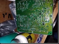
ECU16

ECU back and closed up.

ECU17

Short summary of what I did on the rear casing. I had to substitute some different voltage capacitors based on what I had available.