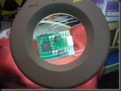
As above, pictures below, those 0402 decoupling capacitors were kinda hard to get in place. A good magnifying glass really speeds things up.
I assembled the LMZ power modules 1st, they have a huge thermal pad on the back that need serious heat to solder them down.
Here’s the rest of the power supply section tested. Then I metered the output voltages, all within design limitations, before I proceeded (1.2v and 2.5v, measured was 1.18v and 2.48v).
Some noise figures, scope was at 0.2mV/div with an X10 probe, 0% load, I need to retest this again at full load and with a better scope, current scope has a bandwidth limit of 20Mhz, which might not be showing everything.
Then I assembled the rest of the stuff, including the Spartan-6 FPGA, I left some of the capacitors around the sides unassembled so I can visually inspect the BGA soldering quality (didn’t take a picture though).
Next I tackled the underside, which has some 0402 decoupling capacitors. These were insanely hard to do naked eyed.
Here’s a closeup comparison with a 0.5mm ball point pen tip.
This is how I did it by hand (mostly), a good magnifier and strong light helps a lot, you don’t want weird shadows obscuring your view.
A shot of the completed board through the magnifier. It looks good doesn’t it?
Here it’s connected to my cheapie Ebay chinese Xilinx platform cable clone, resting on my messy as hell table.


No comments:
Post a Comment